Automotive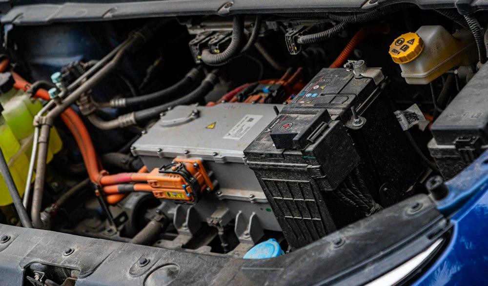
Battery management and ADAS
Heavy-copper power boards and radar modules built to IATF 16949, with PPAP on request.
For automotive, telecom, medical and industrial electronics. Prototype to volume, on the same line.
Laser drilling
“Microvias down to 75 µm, stacked three levels deep.”
Lamination
“Up to 24 layers, held within ±50 µm registration.”
Copper plating
“25 µm hole-wall copper, microvias filled solid.”
Cores, prepreg and foil are pinned, pressed and cured in one vacuum cycle. Then a UV laser drills only the layers that need connecting, and copper fills what it opened.
microvias drilled on this line.Every one positioned from a customer drill file.
panels moved by AGV.Not one of them carried by hand.
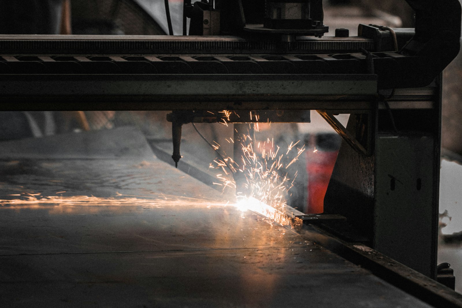
Each hole is placed from your drill file and checked against fiducials on the panel before the laser fires.

Hole walls are plated to 25 µm on average, and microvias are filled so the next layer can stack on top.
Heavy-copper power boards and radar modules built to IATF 16949, with PPAP on request.
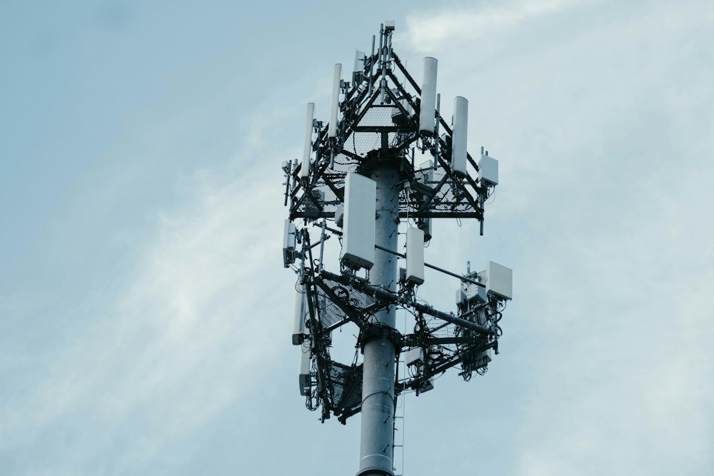
Low-loss laminates, controlled impedance and via fences for RF front ends and arrays.
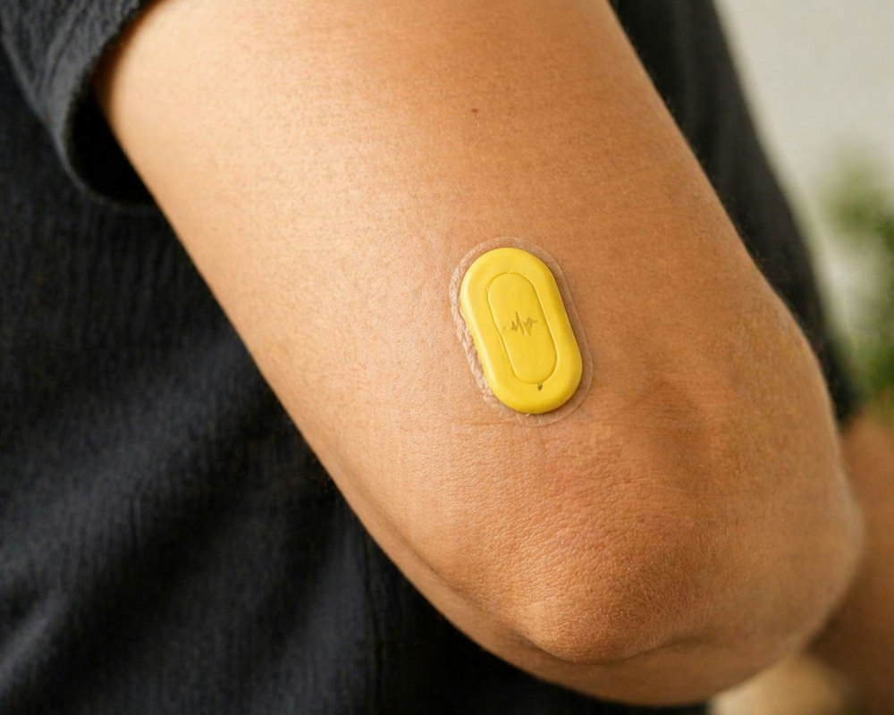
Fine-line rigid-flex for imaging, monitoring and wearable devices, built under ISO 13485.
Autonomous vehicles carry every panel between nine stations on a fixed loop, from inner-layer imaging to electrical test. Each transfer is logged to the panel serial.
The result is simple: no panel waits in a hand-carried queue, and any board can be traced back to its press load and plating tank.
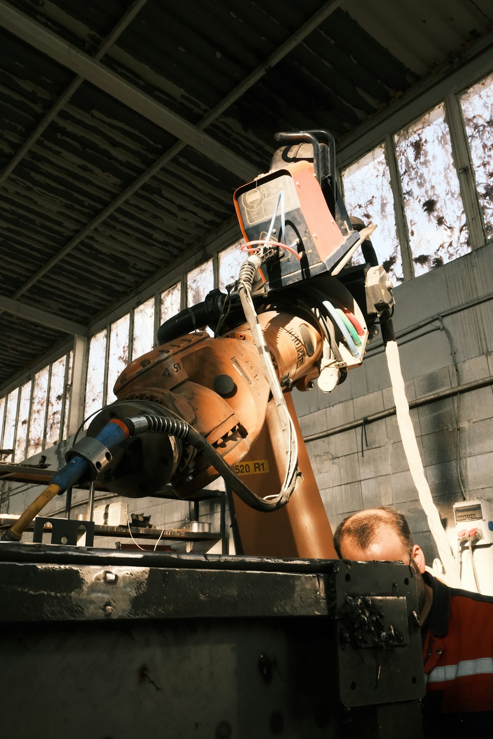
Step 04Vacuum lamination with pin-lam registration
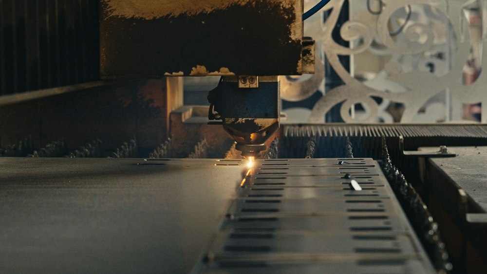
Step 05UV laser drilling at 355 nm

Step 06Electrolytic copper and via fill

Key capabilities.
| Comparison | BRAND line | Typical PCB shop | Broker |
|---|
A few of the questions engineers ask before their first order.